Glass PCB

Geyuan Electronics is a professional glass PCB manufacturer in China with a large production scale. With our experienced purchasing team, PCB engineering team, and advanced manufacturing equipment, we are confident in meeting your various glass PCB needs. Contact us now for a quote.

High-Quality Glass PCB Supplier

Looking for the perfect glass PCB solution? No problem! Leave all the worries to us. Geyuan Electronics has a professional team of engineers and designers to meet all your PCB and other PCB assembly needs. We are developing and innovating a comprehensive range of glass PCB products. Furthermore, our in-house factory boasts over 10,000 square meters of production facilities equipped with advanced production equipment. We are always committed to customer satisfaction and strive to make every customer happy. If you require a specific type of glass PCB, please contact us directly.

Glass PCB professional manufacturer
Precision glass PCB assembly and manufacturing workshop

Professional Glass PCB Manufacturer

For over a decade, we have specialized in the assembly, design, and manufacturing of high-quality PCBs, making us the ideal choice for your upcoming projects and businesses. We offer only the latest and highest quality glass-based printed circuit boards, and we can customize product design and functionality to your requirements. Our expert team is dedicated to finding new ways to improve processes to ensure you receive the highest quality products. We also have a comprehensive quality control system and utilize the latest technologies to ensure our products meet all industry standards. Contact us now to start your glass PCB project.

Custom Glass Printed Circuit Board Capabilities

We offer fully customized glass core PCB one-stop solutions to meet clients’ individualized and differentiated project needs. Customizable core parameters include glass core thickness, overall PCB dimensions, TGV via location, aperture size, aspect ratio, fine line spacing, and multi-layer stacking. We offer a variety of surface treatment options, including gold plating, silver plating, anti-oxidation treatment, and high-frequency low-loss coatings. We can tailor material formulations and manufacturing processes to specific application scenarios such as high frequency, high temperature, high vibration, and high reliability. Flexible production services cover sample customization, small-batch pilot production, and large-scale mass production, fully meeting the needs of high-end electronic equipment’s full-cycle iterative R&D and mass production.

Glass PCBs prototye

Types of Glass PCB

Glass Copper PCB

Glass Copper PCB

Glass copper PCB has approximately 1.66mmboard thickness. It is commonly applicable toelectronics and other applications.
Transparent Glass PCB

Transparent Glass PCB

Available in crystal transparent solder mask. Theclear glass PCB is comprised of aluminum andcopper materials.
Glass Epoxy PCB

Glass Epoxy PCB

We manufacture glass epoxy PCB using high-quality raw materials. This enables rigid and flatsubstrates for this product.
Glass Fiber PCB

Glass Fiber PCB

Glass fiber PCB are flexible substrates that letboards suit complicated spaces. Features a rigiddesign that ensures long-lasting use.
Multilayer Glass PCB

Multilayer Glass PCB

Multilayer glass PCB comes with a uniquedesign. These are highly chemically inactive, canpersist to heat or acids.
Printing Glass PCB

Printing Glass PCB

We offer printing glass PCBs that are highlyresistant to bases, acids, and heat. It has thequality you need for a specific use.
Glass PCB bare board manufacturing process

Key Challenges in Glass PCB Manufacturing

The production of glass PCBs faces two major challenges. Firstly, the number of laser-drilled holes directly impacts manufacturing difficulty. More holes mean longer processing time and a greater risk of precision issues. Therefore, minimizing the number of holes during the design phase is crucial for improving production efficiency and product quality. Secondly, overly complex final product shapes are prone to deformation or breakage, especially during transportation or assembly. To address this, designs should balance functionality and structural integrity, simplifying shapes as much as possible to improve durability and reliability.

Engineering Team and DFM Capabilities

We have a highly experienced professional team. Our engineers and technicians possess years of industry experience and expertise, enabling them to provide comprehensive technical support and solutions for our clients. Whether in the design or production phase, we offer customized services to meet your specific needs. Therefore, we can provide Design for Manufacturability (DFM) review services for your glass PCB manufacturing projects, analyzing potential risks in your design. Furthermore, our DFM goes far beyond basic linewidth checks; it includes structural review, substrate selection review, shape review, interconnect review, and assembly review, as glass presents greater challenges in machining and structural transitions compared to FR-4.

Mass production of glass printed circuit boards

How a Glass PCB Is Manufactured

Glass boards are built with thin-film and panel-level packaging processes, not laminate pressing. The sequence below is the standard double-sided TGV flow.

STEP 01: Substrate Prep

Float or down-draw glass panels are cut, edge-ground and cleaned (RCA / plasma) to particle-free, < 1 nm Ra surfaces.

STEP 02: TGV formation

Laser-induced deep etching (LIDE) or laser drilling + HF etch opens 30–100 µm through-glass vias with crack-free walls.

STEP 03: Seed metallization

Sputtered Ti/Cu (≈ 50/200 nm) coats both faces and via walls, giving adhesion the copper plating will build on.

STEP 04: Photolithography

Dry-film or spray resist is exposed by laser direct imaging — 10 µm lines are routine, < 5 µm with semi-additive plating.

STEP 05: Copper electroplating

Pattern plating grows traces and via fill to 5–20 µm. Pulse plating keeps TGV fill void-free at 10:1 aspect ratios.

STEP 06: Etch & strip

Resist strip and flash seed etch isolate the circuit. The smooth glass interface leaves near-vertical conductor sidewalls.

STEP 07: Surface finish

ENIG or ENEPIG over copper enables SAC reflow and Au wire bonding; OSP serves cost-driven single-side builds.

STEP 08: Singulation & test

Laser cutting or dicing saw separates boards; AOI plus flying-probe electrical test close out the lot.

Glass Printed Circuit Board Quality Inspection

Solving Your Glass PCB Technical Problems

Our in-house technical team is always ready to solve a variety of problems for you, including impedance mismatch, copper foil bonding, custom thicknesses, and much more. We work closely with our clients during the prototyping stage, ensuring a transparent production and delivery process. Instead of waiting for lengthy email exchanges or empty promises, you’ll directly connect with a team that is proficient in layout design and provides concrete process feedback, not generic template responses.

Specialized Glass Printed Circuit Board Production Workshop

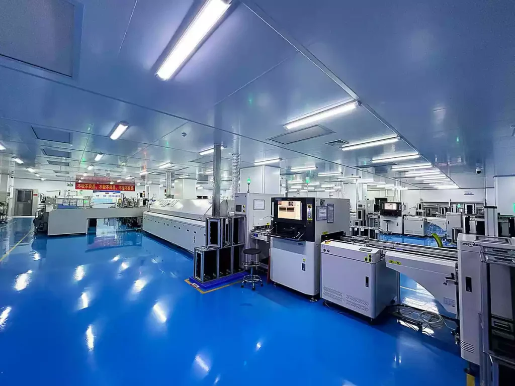
We have tailored our production line to the unique properties of glass. Glass is not a material that can be easily processed like FR4 or polyimide; it requires entirely different handling methods. Therefore, our factory is equipped with laser direct imaging equipment for ultra-fine geometries, specialized glass drilling equipment, and polishing processes to ensure optical clarity. We have optimized our workflows to meet the ever-increasing demands of engineers pushing the limits in signal integrity, heat resistance, and visual design.

Custom production of glass printed circuit boards
Glass based PCB small batch manufacturing services

Glass Core PCB Production Capacity and Equipment

All glass core PCB products are manufactured in Class 1000-10000 cleanrooms to ensure extremely high consistency and purity. The entire production process employs ultra-precision glass thinning and forming techniques, combined with femtosecond laser TGV modification and wet etching technology, to create a uniform, crack-free micropore array. After nanoscale plasma polishing, physical vapor deposition (PVD) seed layer deposition and pulsed copper plating processes are used to form void-free, highly reliable conductive vias. Subsequently, fine linear density regularization (RDL) lithography, precision circuit etching, and professional surface plating treatment are used to construct a high-density, high-precision circuit layer. The entire production process is supplemented by chemical strengthening, edge passivation, and high-precision lamination technologies, effectively ensuring that the finished product has ultra-low warpage, high flatness, and stable and consistent electrical performance.

Customized Glass PCB Manufacturing Services

Every customer has unique needs, making customized services crucial for PCB manufacturers. An excellent customer service team should be able to provide customized solutions based on specific customer requirements, ensuring products meet their demands and expectations. Whether it’s custom design for a specific application area or requirements for special materials and processes, manufacturers should be flexible and responsive to meet individual customer needs. Please contact Geyuan Electronics to customize your PCB. Our independently developed glass PCBs are renowned for their high transparency, flatness, heat resistance, tear resistance, and deformation resistance. This glass circuit board meets our customers’ high standards.

Precision glass PCB prototype supplier

Browse Different PCB Solutions for Every Need

Looking for the right PCB solution? Explore various types of PCBs to find the perfect match for your project.

Aluminum PCB

Aluminum PCB

PCBs with aluminum metal core for efficient heat dissipation in high‑power designs.
Single sided Rigid PCB

Rigid PCB

Standard rigid FR4 boards offering stable structure for general electronic systems.
Copper‑Core PCB

Copper‑Core PCB

Metal‑core PCB with copper base for superior thermal conductivity and heat spreading.
High TG PCB

High-TG PCB

PCBs made with high glass transition temperature (Tg) materials, typically 170°C and above.
High Frequency PCB

High Frequency PCB

PCBs designed to handle signals in the GHz range with minimal signal loss and distortion.
High Speed PCB

High Speed PCB

Circuit boards optimized for high-speed digital signals with careful attention to signal integrity.
HDI PCB

HDI PCB

High Density Interconnect PCBs with finer lines, smaller vias, and higher connection density.
Rogers PCB

Rogers PCB

PCBs manufactured using Rogers Corporation's high-performance laminate materials.
Heavy Copper PCB

Heavy Copper PCB

PCBs with exceptionally thick copper layers, typically 3 oz or more, for high-current applications.
Flexible PCB

Flexible PCB

Bendable PCBs made with polyimide or polyester substrates for dynamic or space-constrained designs.
Rigid Flex PCB

Rigid-Flex PCB

Hybrid circuit boards that combine rigid and flexible substrates into a single integrated assembly.
Ceramic PCB

Ceramic PCB

Using ceramic substrates like Al₂O₃ and AlN for extreme thermal and electrical performance.
Precision glass PCB manufacturing workshop

Comprehensive Glass PCB Solutions

The most successful strategy in glass PCB manufacturing is to treat prototyping, assembly planning, and production planning as a whole, rather than separate decisions. The first prototype can be used to confirm the structure, routing, interconnect compatibility, or assembly readiness. Afterward, the project can move to the engineering sample stage or be repeated according to a more stable production plan. Therefore, assembly planning should begin as early as possible, also because the handling of glass substrates is significantly different from FR-4 substrates. Support methods, edge protection, fixture strategies, and mounting conditions all affect yield and reliability. This is especially important when the substrate is thin, transparent, optically sensitive, or requires support for heat transfer.

Glass PCB Prototyping and Mass Production Services

Geyuan Electronics offers comprehensive glass PCB (Printed Circuit Board) manufacturing and prototyping services, transforming your innovative ideas into functional prototypes and high-quality, production-ready PCBs. Our team works closely with clients to develop prototypes and scale to full production, ensuring quality and efficiency at every stage. By partnering with Geyuan Electronics, you gain access to a team dedicated to providing high-quality PCB manufacturing and PCB prototyping solutions, driving innovation and success. We focus on superior quality and customer satisfaction, ensuring your project succeeds in today’s competitive market.

Custom production of precision glass printed circuit boards
Custom glass PCB manufacturing

Quality and Testing Standards

All glass-core PCB products strictly adhere to IPC industry standards, AEC-Q100 automotive-grade specifications, aerospace-grade reliability requirements, and other high-standard industry standards. We have established a comprehensive product testing and verification system to ensure product stability and reliability. Routine reliability testing includes high and low temperature cycling, thermal shock, high-temperature aging, damp heat, mechanical vibration, and impact testing. In addition, we conduct professional performance verifications such as high-frequency electrical performance testing, impedance consistency testing, warpage detection, and insulation breakdown testing. End-to-end quality control ensures stable signal transmission, zero delamination, and zero functional failures under extremely complex operating conditions.

Our Quality Management System and Certification Standards

We have an excellent customer service team that strictly implements the quality management system to ensure stable and reliable product quality that meets customer requirements and standards. From raw material procurement to manufacturing and final delivery, the manufacturer conducts rigorous quality control and inspection to ensure that every batch of products meets the highest quality standards. Furthermore, we ensure that every glass PCB undergoes strict inspection and testing before delivery to guarantee its reliability. Since our inception, we have guaranteed that our PCBs have passed REACH, RoHS, ISO14001:2015, UL (E477880), and ISO9001:2015 certifications.

Precision glass PCB supplier

Types of Glass Materials Used in Glass PCBs

Glass materials are mainly divided into two categories. There are also two main types of glass used in glass PCBs: fiberglass reinforced epoxy glass and bare glass. There are three types of crystalline glass that can be used in glass PCBs.

Glass Copper

Glass Copper

Our glass copper PCBs are high-quality products widely used in electronics and hobby applications. We offer a variety of sizes and thicknesses to meet your specific needs.
Glass

Glass Epoxy

Glass epoxy is ideal for electronic applications with high demands for reliability, design flexibility, and cost-effectiveness. These boards are made with high-quality glass epoxy, significantly enhancing product strength.
Glass Fiber

Fiberglass

Fiberglass PCBs feature a moisture-proof design, enabling them to withstand harsh environments. Furthermore, they have a low thermal shrinkage rate and a low coefficient of thermal expansion, providing highly durable and protective circuitry.
Tempered Glass

Tempered Glass

A printed circuit board with a tempered glass surface and a thin layer of plastic laminated on top. This makes the PCB structure stable and durable when applied to a variety of devices and electrical appliances.
Quartz Glass

Quartz Glass

Quartz glass is the best choice for surface mount technology and leaded chip through-hole layouts. Each circuit board's unique surface treatment process provides superior solderability, excellent continuity, and outstanding electrical performance.
Sapphire Glass

Sapphire Glass

Among various glass materials, sapphire glass has the highest heat resistance and the lowest gas release rate of all glass substrates. Its optimal coefficient of thermal expansion makes it ideal for modern complex circuit boards.

Key Applications and Service Industries

Glass core PCB technology is driving innovation in several high-growth sectors:

Instrumentation Products

Display Revolution

Transparent displays (advertising, smart windows), OLED/QLED/Micro-LED electrodes/backplanes enabling under-display cameras and sensors in smartphones.
AI industry

Next-Generation Consumer Technology

Foldable/rollable phone hinges and interconnect technologies, transparent device concepts, smart home control panels on glass/mirrors.
Wearable Technology

AR/VR Glasses

Mounting displays and sensors directly on transparent lenses/waveguides without obstructing the user's view. This is crucial for mass adoption.
New Energy

Solar Energy

Transparent electrodes for thin-film solar cells.
LED Smart Systems

Smart Buildings

Windows integrating display, lighting, or heating functions.
Medical Electronics

Medical Devices

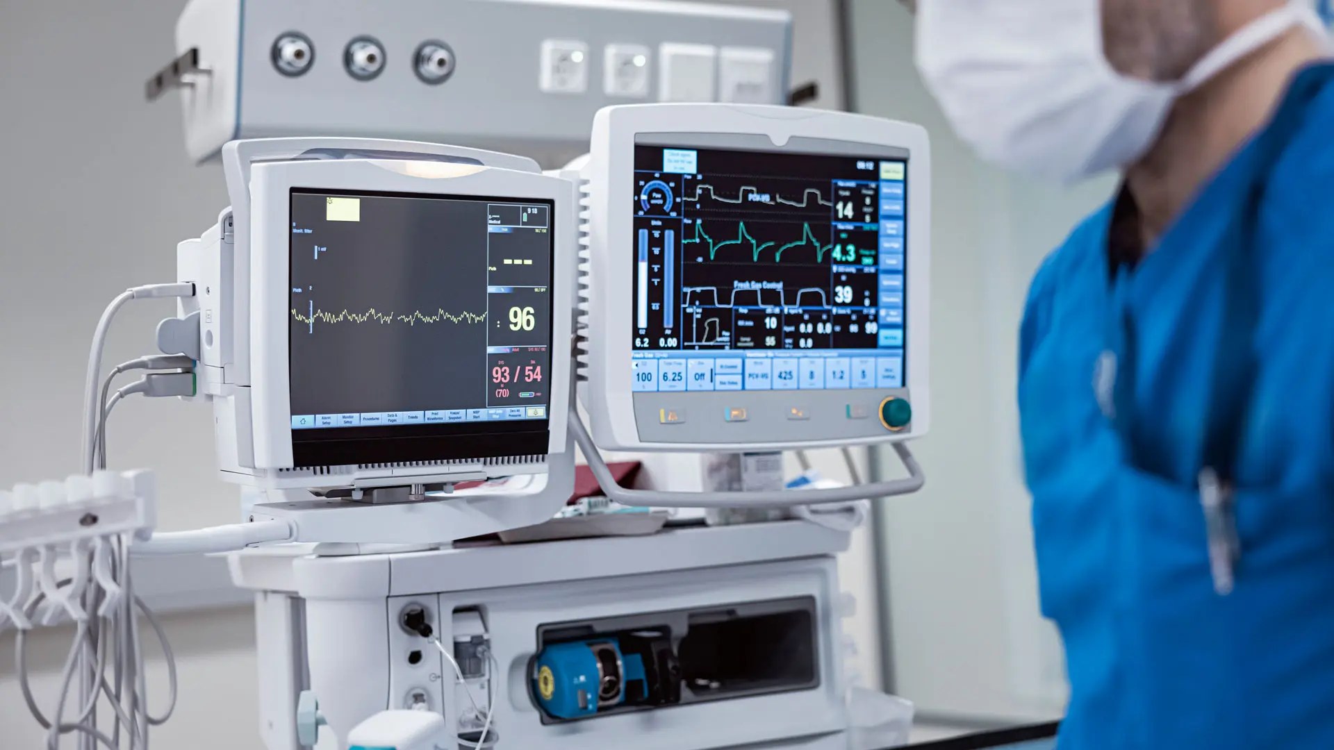
Transparent sensors for imaging or patient monitoring interfaces.

FAQ

This type of printed circuit board is made using a glass substrate (borosilicate glass, fused silica glass, soda-lime glass, or sapphire glass) instead of FR-4 laminate. Copper conductors are deposited on the glass substrate through sputtering and electroplating processes, creating a very smooth, fine circuit on a flat, transparent, and dimensionally stable medium.

Prototype production costs are approximately 5-20 times that of FR-4 boards: 10 50×50 mm double-sided borosilicate boards cost approximately $45-$120 each, plus $300-$700 for mold costs. If using soda-lime glass boards for panel-level mass production, the cost per board can be less than $5. Please use the T-03 estimator above to calculate your geometry.

Components can be attached using soldering, conductive adhesive, wire bonding, flip-chip bonding, or other packaging methods. The specific process used depends on pad surface treatment, component type, and thermal requirements.

Thin-film lithography typically achieves linewidths/spacings of 10–50 µm, while semi-additive processes can achieve below 5 µm. Printed or laser-structured conductors are larger, ranging from 75–150 µm. Sub-nanometer glass surfaces significantly reduce conductor edge roughness, thereby substantially reducing RF losses.

Through-Glass Vias (TGVs) are formed by first using laser-induced deep etching (LIDE) or laser drilling, followed by hydrofluoric acid (HF) etching, and finally metallization through sputtering of a seed layer and copper plating. Typical diameters are 30–100 µm, with spacing up to 150 µm and an aspect ratio of approximately 10:1.

The main cost factors include glass material, substrate size, thickness, number of TGVs, via size, circuit density, metallization, surface finish, testing requirements, and production quantity.

Ready To Start Your Next Custom Glass PCB Project?

From concept to production, let our engineering team bring your vision to life. In addition to PCB manufacturing, we offer comprehensive electronics services, including PCB design, PCBA (Printed Circuit Board Assembly), and turnkey solutions. Whether you need assistance with prototyping, design verification, component sourcing, or mass production, we provide end-to-end support to ensure your project's success. For PCBA services, please provide your Bill of Materials (BOM) and any specific assembly instructions. We also offer DFM/DFA analysis to optimize your design, improving its manufacturability and assemblability, thus ensuring a smooth production process.

Call to Actions1
Scroll to Top