HDI PCB

As a professional HDI PCB manufacturer, Geyuan Electronics provides HDI PCB manufacturing services for compact, high-speed, high-density electronic products. We support microvias, blind vias, buried vias, through-hole vias, multilayer HDI structures, DFM auditing, impedance control, reliable manufacturing processes, and optional PCB assembly services, helping engineers build advanced circuit boards faster and with greater confidence. Whether you need prototyping or high-volume manufacturing, we can provide the services. Contact us now for a free quote.

Fast and Reliable HDI PCB Manufacturing and Assembly Services

Looking for an HDI PCB manufacturer that provides accurate, fast, and reliable delivery, avoiding delays and high rework costs? Geyuan Electronics, with over 20 years of experience, AS9100 Rev-D and ISO 9001:2015 certified processes, and advanced production facilities in Dongguan and Shenzhen, China, is committed to providing high-quality HDI PCB manufacturing and assembly services for complex, high-performance applications. Whether you need rapid HDI PCB prototyping or comprehensive HDI PCB electronics manufacturing, we can help you build smarter, more efficiently, and with more confidence.

HDI PCB mass production

One-Stop HDI PCB Manufacturing Service

If you want to save yourself the hassle, you can choose our one-stop turnkey service. We can handle the entire process, including material selection, PCB design, HDI PCB manufacturing and assembly, as well as packaging and shipping. All you have to do is wait for the goods to arrive.

HDI circuit boards Engineering Led DFM Support

Engineering-Led DFM Support

Geyuan Electronics' engineering team reviews Gerber files, stack-up requirements, via structures, material selection, copper foil weight, impedance requirements, and manufacturability risks before production. This helps reduce design modifications and supports a smoother HDI PCB manufacturing process.
Experience in Advanced HDI Structures

Experience in Advanced HDI Structures

Our manufacturing team provides support for high-density PCB design, including microvias, blind vias, buried vias, sequential lamination, via filling, and fine routing. These capabilities are crucial for high-density PCB applications where routing space and signal quality are critical.
High end multilayer HDI circuit board Rapid Prototyping to Production Support

Rapid Prototyping to Production Support

Geyuan Electronics supports rapid PCB prototyping, small-batch orders, and mass production manufacturing. This enables engineering teams to quickly validate HDI PCB designs and rapidly scale to stable production levels after design completion.
HDI PCB Quality Control Throughout the Entire Process

Quality Control Throughout the Entire Process

From incoming raw material inspection to imaging, drilling, electroplating, lamination, AOI (Atomic Force Microscopy), electrical testing, and final inspection, Geyuan Electronics implements rigorous process control at every stage of manufacturing. This ensures high reliability, meeting the demands of demanding electronic applications.
HDI PCB Support for High Speed ​​and High Frequency Designs

Support for High-Speed ​​and High-Frequency Designs

HDI PCBs are commonly used in high-speed communications, RF, and high-frequency products. Geyuan Electronics supports impedance control, appropriate laminate selection, and precise manufacturing control to ensure consistent electrical performance.
HDI PCB One Stop PCB and PCBA Services

One-Stop PCB and PCBA Services

For customers requiring complete project support, Geyuan Electronics offers bare board manufacturing and PCB assembly services. This helps reduce supplier coordination and improves project efficiency from PCB manufacturing to finished product assembly.
hdi pcb for small components

Designed for Next-Generation Electronics: HDI PCBs

Everything Geyuan Electronics does boils down to one question: How do we help innovators push the boundaries of design? For us, High-Density Interconnect (HDI) represents the pinnacle of our work. With over 20 years of experience, AS9100D/ISO certified processes, and award-winning on-time delivery, we have earned the trust of engineers across various fields. From the first prototype to full-scale production, our team manufactures HDI boards with the same precision and reliability, serving over 30,000 customers worldwide.

HDI PCB Technical Capabilities

Geyuan Electronics supports HDI PCB manufacturing based on IPC Class 2 and Class 3 requirements. The specifications below help customers evaluate our manufacturing capabilities for complex HDI PCB projects.

Layer Count1–40 Layers
HDI Build-Up1+N+1, 2+N+2, 3+N+3, 4+N+4, Any-Layer HDI
Board Thickness0.037 mm – 6.5 mm
Board Dimension1–2 Layers: 1500 × 600 mm; Multilayer: 620 × 720 mm
Minimum Laser Microvia0.08 mm
Minimum Mechanical Drill0.15 mm
Aspect RatioStandard 25:1; Max. 35:1
Blind Via Aspect Ratio0.8:1
Base MaterialsFR4, Halogen-Free, Metal Core, Polyimide, High-Frequency Materials, Mixed Lamination
FR4 Tg OptionsTg 140, Tg 170, Tg 180
High-Frequency MaterialsRogers 4350B, 3003, 4003C, 5880; Taconic; Teflon
Material BrandsKB, ITEQ, Shengyi, Isola, Rogers, Ventec, Panasonic, Taconic, Nelco, Bergquist, DENKA, or customer-specified laminates
FlammabilityUL 94V-0
Thermal Conductivity0.3–400 W/m·K, depending on material type
Minimum Trace / Space64 μm / 64 μm
Line Width / Space Tolerance±0.015 mm
Minimum Annular Ring50 μm
Minimum Pad-to-Pad Clearance40 μm
Layer-to-Layer Registration≤100 μm
Solder Mask Registration≤38 μm
Minimum Solder Mask Clearance2 mil
Solder Mask Dam50 μm
Copper Thickness1/3 oz – 33 oz
Surface FinishesHASL Lead-Free, ENIG, OSP, Immersion Silver, Immersion Tin, Hard Gold, Gold Fingers, Carbon Ink, Bare Copper
Solder Mask ColorsGreen, White, Black, Blue, Red, Yellow, Orange, Purple, Matte Green, Matte Black
Solder Mask BrandsRongDa, KuangShun, Coants, LanBang, Taiyo
Solder Mask Thickness0.2 mil – 1.6 mil
Via Plugging0.2 mm – 0.8 mm
Board Thickness Tolerance±5%
Hole Diameter Tolerance±0.05 mm
Hole Location Tolerance±2 mil
Outline Tolerance±0.1 mm
V-Cut Tolerance±10 mil
Beveled Edge Tolerance±5 mil
Impedance Tolerance50Ω, ±10%
Warp and Twist≤0.50%
Quality StandardsIPC Class 2 / Class 3
Quality TestingAOI, 100% Electrical Test
Advanced Via ProcessesBlind Vias, Buried Vias, Laser Microvias, Via-in-Pad, Resin Plugged Vias
Mechanical FeaturesCastellated Holes, Press-Fit Holes, Countersink / Counterbore Holes, Edge Plating
Special PCB ProcessesThick Copper, Copper Block Embedded, Z-Axis Milling, Gold Fingers, Carbon Ink, Peelable Solder Mask
High-Frequency SupportHigh-Frequency Materials, High-Frequency Mixed Lamination, Foam Board
Engineering ServicesDFM Check, Stack-Up Review, Impedance Review
Expedited Production24-Hour Expedited Production Available
Data FormatsGerber, DXF, PCBdoc, ODB++, HPGL, BRD
Any Layer HDI PCB Fabrication

HDI PCB Engineering and Design Capabilities

Early Engineering Review for HDI Projects

Once you send us your Gerber files, BOM, stacking diagrams, and project requirements, our engineers will review key manufacturing details, discuss any concerns with you, and confirm a clear production plan before proceeding.

DFM and Impedance Modeling

We conduct comprehensive DFM reviews of HDI PCB designs to minimize rework and manufacturing defects. We offer impedance modeling services to ensure PCB trace dimensions and spacing meet requirements, which is crucial for high-speed signal applications.

Signal Integrity Review

We provide signal integrity review services for high-speed circuit designs to prevent signal loss and distortion in high-frequency applications. We evaluate trace layout, via placement, stack-up structure, and other factors to optimize high-speed circuit designs. We use advanced simulation tools and time-domain reflectometry (TDR) for in-depth signal integrity analysis.

In-Pad Via Design Support

We help engineers improve routing efficiency and optimize board space utilization through in-pad via design support. This ensures design robustness and manufacturability.

Cleanroom treatment and AOI technology for features below 75µm

We use cleanroom treatment for HDI PCBs to eliminate the possibility of contamination. We use AOI technology to detect problems such as incorrect component placement.

Your Trusted HDI PCB Manufacturer

With modern factories in Dongguan and Shenzhen, China, we are a leading HDI PCB manufacturer, continuously investing in state-of-the-art production and testing equipment and technologies. At Geyuan Electronics, we possess deep engineering experience, enabling us to complete complex projects on time and within budget with remarkable precision. Our manufactured HDI PCBs feature finer lines, smaller spacing, and denser wiring, which not only enables faster connection speeds but also reduces project size and volume. These boards also utilize technologies such as blind and buried vias, laser-drilled microvias, sequential lamination, and in-pad vias. Furthermore, we employ state-of-the-art equipment and technologies, including laser direct imaging, to maintain tight tolerances that meet the demands of today’s HDI PCBs.

HDI PCB Engineers are inspecting film boards

HDI Board Types We Manufacture

Through years of relentless research and development and technological advancements, Geyuan Electronics has become a benchmark enterprise in the field of rapid manufacturing of small- and medium-batch HDI PCBs. From the initial 1+N+1 and 2+N+2, to 3+N+3, and now to 5+N+5/6+N+6/7+N+7, we have successfully transformed from rapid prototyping to stable mass production, and built a highly respected brand image through our unwavering pursuit of superior quality.

1N1 HDI

1+N+1 HDI

Single buildup layer on both sides of the core. 1+0+1, 1+1+1 configurations. Most cost-effective HDI solution.
2N2 HDI PCB Structure

2+N+2 HDI PCB Structure

This stack-up involves 2 build-up layers on both sides which leads to 4 additional layers in stack-up and offers 2 consecutive layers for HDI connections. So, the complexity of the design increases the build-up layer count increases. But these stack-ups won’t use stacked vias.
ELIC Stack up

ELIC Stack-up

Every layer interconnect (ELIC) stack-up offers all the layers in the stack-up to act like HDI layers and uses filled micro stacked vias to complete the interconnections in any layers. This stack-up gives excellent electrical reliability with interconnections.
3N3 HDI PCB Structure

3+N+3 HDI PCB Structure

The 3+N+3 HDI structure is designed for ultra-high density interconnect applications requiring maximum routing capability and vertical interconnect performance.
Any Layer HDI

Any-Layer HDI

Sequential lamination allowing vias on any internal layer. Maximum routing density and design flexibility.
Substrate Like PCB

Substrate-Like PCB

SLP technology with even finer line/space than traditional HDI. Feature sizes approaching IC substrate levels.
Staggered Via HDI PCB

Staggered Via HDI PCB

This type of HDI PCB uses interlaced microvias, achieving a more compact and efficient design through drilling at varying depths and sizes. Interlaced through-hole designs are particularly suitable for high-speed applications requiring precise signal routing.
Stacked Via HDI PCB

Stacked Via HDI PCB

This type of HDI PCB uses stacked microvias, interconnected by drilling multiple layers and using conductive materials. Stacked through-hole designs can accommodate higher circuit density than interlaced through-hole designs.
Flexible HDI PCB

Flexible HDI PCB

This type of HDI PCB combines the advantages of HDI technology with the flexibility of flexible PCBs. Flexible HDI PCBs are commonly used in applications with strict space and weight requirements.
High density HDI PCB laser hole microvia PCB manufacturer

High-Performance, High-Density Solutions for Advanced Applications

High-density interconnect (HDI) PCBs offer numerous high-density features, including laser-drilled microvias, sequential lamination structures, fine-line wiring, and high-performance thin materials. This high density enables more functionality per unit area. Advanced HDI PCBs utilize multi-layer copper-filled stacked microvias to create structures that allow for more complex interconnects. These complex structures provide the necessary routing and signal integrity solutions for the high-pin-count, small-pitch, and high-speed chips in today’s high-tech products. With over 20 years of experience in electronics manufacturing and more than 152,000 completed projects, Geyuan Electronics provides comprehensive support from HDI PCB manufacturing to PCBA and complete system assembly, helping customers transform advanced HDI designs into reliable, mass-producible electronic products.

HDI PCB Fabrication & Assembly Built Around Your Needs

HDI PCB Fabrication

HDI PCB Fabrication

As a leadi-density multilayer boards with microvias, blind/buried vias, and fine trace routing for maximum performance.
HDI PCB Assembly

HDI PCB Assembly

Our HDI PCB assembly services ensure precise component placement, strong interconnections, and fully tested boards ready for deployment.
HDI PCB Prototype

HDI PCB Prototype

Need fast validation? Our HDI PCB prototype services help you test, refine, and accelerate your product development.
Full HDI PCB Electronics Manufacturing

Full HDI PCB Electronics Manufacturing

We provide complete HDI PCB electronics manufacturing, including design support, fabrication, assembly, and testing all under one roof.
hdi PCB CNC drilling

Work With Us Early On Your HDI PCB Project

Compared to standard circuit boards, HDI designs allow for less late-stage modification, making early collaboration one of the wisest decisions for your project. Our engineers will work with your team before production begins: reviewing the stack-up, collaboratively developing design rules, identifying design-for-manufacturability (DFM) issues, and recommending materials that balance performance, manufacturability, and budget. Whether you are in the early stages of development, extending an existing design, or applying for regulated industry certification, we can support you at every stage.

Order HDI PCBs And Assemble Online

We offer transparent pricing with no hidden fees. Our products are all manufactured in our own factory, so you can use them with confidence. Contact us now for a quote.

Call to Actions1
HDI PCB production

Superior Quality HDI PCBs

We have earned an excellent reputation for our superb PCB manufacturing processes. Our strong custom PCB manufacturing capabilities allow you to obtain high-quality HDI PCBs at highly competitive prices, with no minimum order quantity. Our team will conduct a manufacturability design check on your custom PCB files and communicate with you to ensure that the files meet production requirements and that the board meets your performance specifications. Furthermore, we have an in-house quality control department that rigorously monitors finished products to ensure they meet your high quality standards.

Fast Turnaround HDI PCB Manufacturing

If you have an HDI PCB manufacturing project that requires urgent completion, Geyuan Electronics is the ideal choice. We possess exceptional fast PCB manufacturing capabilities, including top-tier engineers and advanced technology, enabling us to meet your stringent project deadlines and budget requirements. Depending on the complexity of your project, we can complete PCB manufacturing in as little as 24 hours.

HDI PCB SMT assembly production workshop

Browse Different PCB Solutions for Every Need

Looking for the right PCB solution? Explore various types of PCBs to find the perfect match for your project.

Aluminum PCB

Aluminum PCB

PCBs with aluminum metal core for efficient heat dissipation in high‑power designs.
Single sided Rigid PCB

Rigid PCB

Standard rigid FR4 boards offering stable structure for general electronic systems.
Copper‑Core PCB

Copper‑Core PCB

Metal‑core PCB with copper base for superior thermal conductivity and heat spreading.
High TG PCB

High-TG PCB

PCBs made with high glass transition temperature (Tg) materials, typically 170°C and above.
High Frequency PCB

High Frequency PCB

PCBs designed to handle signals in the GHz range with minimal signal loss and distortion.
High Speed PCB

High Speed PCB

Circuit boards optimized for high-speed digital signals with careful attention to signal integrity.
Rogers PCB 1

Rogers PCB

PCBs manufactured using Rogers Corporation's high-performance laminate materials.
Heavy Copper PCB

Heavy Copper PCB

PCBs with exceptionally thick copper layers, typically 3 oz or more, for high-current applications.
Flexible PCB

Flexible PCB

Bendable PCBs made with polyimide or polyester substrates for dynamic or space-constrained designs.
Rigid Flex PCB

Rigid-Flex PCB

Hybrid circuit boards that combine rigid and flexible substrates into a single integrated assembly.
Ceramic PCB

Ceramic PCB

Using ceramic substrates like Al₂O₃ and AlN for extreme thermal and electrical performance.
HDI PCB production factory

We Offer Low-cost HDI PCB Manufacturing Services

Geyuan Electronics provides the highest quality HDI PCB manufacturing services at a low cost. This commitment makes us a trusted PCB manufacturing and assembly service provider in China. We have an experienced team of experts and advanced infrastructure to ensure fast delivery of high-quality products. Are you interested in our HDI circuit board manufacturing services? Do you need fast delivery of full or partial HDI circuit board manufacturing services? Request a free quote online now. Our PCB assembly and manufacturing services operate 24/7 to meet stringent delivery deadlines. Our customer support team is also quick to respond to customer needs.

Geyuan Electronics' HDI PCB Manufacturing and Testing Equipment

Geyuan Electronics has an in-house production facility in Shenzhen and Dongguan, China, covering 12,400 square meters, including a 2,600-square-meter cleanroom, 5 SMT production lines, and 3 DIP production lines. We are equipped with precision drilling machines, electroplating systems, and etching equipment for accurate circuit patterning, as well as reflow soldering machines and wave soldering systems. Our advanced X-ray and AOI equipment ensures high-quality PCB production. Furthermore, our company is constantly seeking development; as an HDI PCB supplier, we have introduced many advanced equipment and actively developed new manufacturing and assembly technologies to produce a variety of complex and precision PCBs to meet diverse customer needs.

HDI PCB manufacture

HDI PCB Assembly Services

SMT Assembly

We deliver high-precision PCB assembly using Surface Mount Technology, perfect for compact and high-performance solutions.

Consigned Components or Turnkey PCB Assembly

We provide flexible options, whether working with your supplied components or offering full turnkey solutions, including sourcing, assembly, and delivery.

Custom PCB Assembly

We deliver personalized PCB assembly services designed to meet your specific project needs and design requirements.

Quick Turn PCB Assembly

We offer fast and efficient PCB assembly with short turnaround times, ensuring top-quality results.

IPC Class 3 PCB Assembly

We produce PCB assemblies that meet rigorous IPC Class 3 standards, ideal for critical applications in aerospace, medical, and other high-reliability industries.

All IC Packages PCB Assembly

We handle the precise assembly of all IC package types, including BGAs, POPs, CGAs, QFNs, DFNs, and CSPs, with consistent reliability.

HDI PCB Manufacturing Process

Customized HDI PCB Manufacturing Solutions for Specific Needs

If you’re struggling to find an HDI PCB manufacturer that meets your specific specifications, Geyuan Electronics’ team of professional process engineers is ready to assist you. We work closely with you to create tailored HDI solutions, ensuring manufacturability, reliability, and performance. Whether it’s highly customized material stack-up structures or complex via configurations, we can bring your ideas to life.

Advanced Manufacturing Technologies

These advanced manufacturing capabilities allow us to produce HDI PCBs with exceptional quality and consistency for industrial applications where reliability is paramount. Our continuous investment in manufacturing technology keeps us at the forefront of HDI capabilities.At our manufacturing facilities, we employ state of the art equipment specifically optimized for HDI production:

  • Precision Laser Drilling Systems: Our ESI and Hitachi laser drilling systems achieve microvia diameter tolerance of ±20μm with exceptional positioning accuracy
  • Advanced Imaging Equipment: LDI (Laser Direct Imaging) systems with 15μm line resolution capability
  • Sequential Lamination Presses: Computer controlled lamination with ±25μm layer to layer registration
  • Automated Optical Inspection: 100% inspection of microvia formation and trace integrity
High density HDI PCB laser via PCB stacked via PCB prototype

HDI PCB Material Options

Material selection plays a crucial role in the reliability, signal performance, thermal stability, and production yield of HDI PCBs. Geyuan Electronics can help customers select the appropriate materials based on operating environment, signal speed, Tg requirements, loss requirements, number of layers, and cost targets.

High Tg FR-4

Suitable for many high-density and multilayer HDI PCB applications that require better heat resistance than standard FR-4.

Low-Loss High-Speed ​​Laminates

Used for high-speed digital designs, communication equipment, servers, and products sensitive to signal integrity.

High-Frequency Materials

Suitable for RF, microwave, antenna, and 4G/5G communication applications.

Halogen-Free Materials

Used for applications requiring compliance with environmental regulations or meeting specific customer material requirements.

Thin Core Materials and Prepregs

Support fine stack-up control and compact HDI layer structures.

Copper Foil Options

Available based on current carrying capacity, impedance, thermal properties, and manufacturing requirements.

Sequential Lamination Cycles

Quality Control Measures

These rigorous quality measures ensure that industrial clients receive HDI PCBs that meet or exceed IPC Class 2 and Class 3 requirements. For critical industrial applications, we can implement additional customized testing protocols to verify specific performance parameters. Our HDI PCB manufacturing incorporates comprehensive quality verification at every stage:

1. Incoming Material Inspection: Verification of critical material parameters
2. Laser Drill Quality Verification: Optical inspection of via diameter and positioning
3. Cross Section Analysis: Regular sampling for microvia formation quality
4. Electrical Testing: 100% test

ing with specialized flying probe equipment for fine pitch HDI
5. 3D X-Ray Inspection: Internal layer registration and hidden feature verification
6. Impedance Testing: Verification of controlled impedance traces

Inspection & Testing Methods

  1. 100% AOI: After Each Lamination Cycle,Layer-by-layer optical inspection
  2. 100% Electrical Test: Flying Probe, All nets, every board
  3. X-Ray: Microvia Registration Verification, Stacked via alignment check
  4. Microsection: Microvia Plating, Cu thickness per IPC-6016 Class B/C
  5. TDR Impedance Verification, ±5% on all controlled structures
  6. Via-Fill Planarisation Check, Surface profile profilometry
  7. Bow and Twist, IPC-TM-650 2.4.22
  8. Laser Via Depth: SEM Cross-section,On qualification lots
Multilayer HDI circuit board products
turn key hdi pcb prototyping

Highest Industrial Quality Certification Standards

All our production and operations are conducted in accordance with the latest quality management systems, such as ISO 9001, ISO 13485, and TS 16949. Furthermore, all our PCBs meet IPC-A-600 Level 2 standards, and, depending on the requirements of specific industrial sectors, Level 3 or 3A standards. For example, medical and automotive products require Level 3 standards, while aerospace products require Level 3A standards. Therefore, we supply HDI PCBs globally and hold ISO 9001, IATF 16949, and IPC Level 3 certifications.

Are You Looking For Cutting-edge PCB Solutions That Can Revolutionize Your Electronic Designs?

Look no further! Geyuan Electronics is your one-stop shop for Highly Developed Innovative (HDI) PCBs that will bring your circuits to life and help you succeed in every project. Choosing Geyuan Electronics as your HDI PCB manufacturer means partnering with a team passionate about helping you succeed. We will go to great lengths to understand the unique needs of your projects and deliver customized solutions that exceed your expectations. With our highly developed innovative technology, you can ensure that your circuits thrive with unparalleled efficiency and reliability, setting new standards for your industry.

HDI Printed Circuit Board Structure

Industry Applications of HDI PCB

Telecommunications

Telecommunications Equipment

HDI PCBs for 4G/5G RF modules, base stations, antenna systems, routers, and high-speed networking devices.
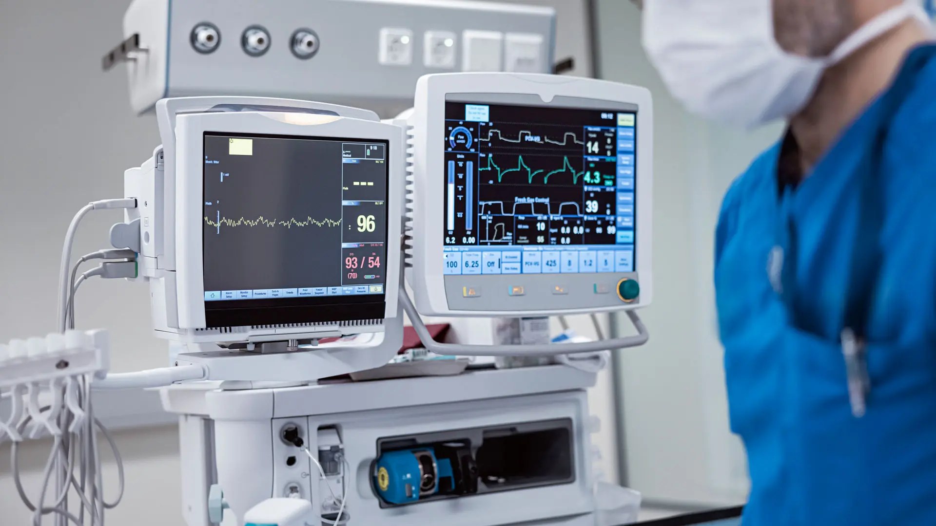
Medical Electronics

Medical Devices

Compact and reliable HDI boards for diagnostic equipment, monitoring systems, imaging devices, and medical control modules.
Smart Home Systems.jpeg

Audio & Video Products

High-density boards for audio processors, cameras, display modules, video transmission systems, and multimedia devices.
drones

Drones

Lightweight HDI PCBs for flight controllers, communication modules, navigation boards, camera systems, and power management units.
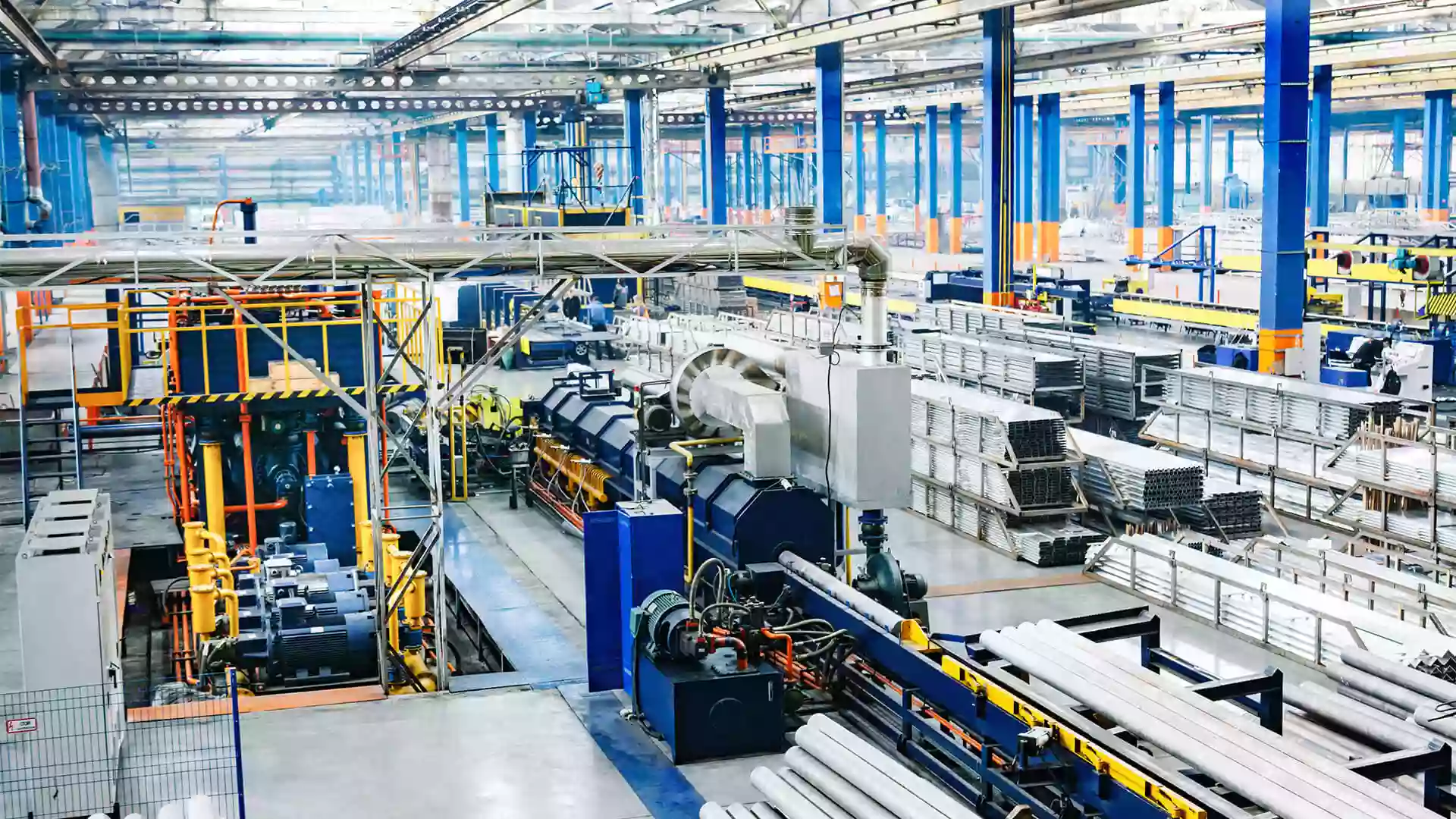
Industrial Equipment industry

Industrial Control

Durable HDI boards for robotics, automation controllers, sensors, printers, laser machines, and industrial communication systems.
Semiconductors

Semiconductors

High-density interconnect boards for IC testing, chip evaluation, burn-in testing, interface boards, and advanced device development.

FAQ

Standard HDI (1+N+1 or 2+N+2) only allows microvias on the outermost stack layer—internal layers are still connected using vias. Arbitrary-layer HDI allows microvias between any two adjacent layers, providing complete routing freedom without needing vias on every layer. Arbitrary-layer HDI can meet the routing density requirements of 0.35–0.4 mm pitch BGAs.

Yes. 0.35 mm pitch BGA fan-out requires in-pad vias, copper fill, and planarization. Our process creates a flat, solderable surface directly above the microvias, compatible with standard solder paste printing and reflow soldering processes. 0.4 mm pitch fan-out is routinely implemented in all arbitrary-layer HDI packages.

For HDI boards, the recommended surface treatment is electroless nickel immersion gold (ENIG). It provides a flat, solderable surface, is compatible with 0.35mm pitch BGA packages, and is suitable for skin contact applications. For applications requiring wire bonding in addition to SMT surface mount technology, palladium-plated electroless nickel immersion gold (ENEPIG) is recommended.

Our standard minimum laser via diameter using CO2 or UV lasers is 0.10 mm, with a positioning accuracy of ±15 microns. For special application requirements, please consult our engineering team. The minimum via pad diameter is typically 0.25 mm (0.10 mm via + 0.075 mm annular pads on each side).

We support up to 6 consecutive lamination cycles, corresponding to up to 30 layers in any layer HDI structure. Each cycle adds a pair of molding layers. Most HDI designs for mobile and wearable applications use 2-4 cycles (8-14 layers in total).

High-density interconnect (HDI) PCBs utilize fine traces, small vias, microvias, blind vias, buried vias, and compact multilayer structures to achieve higher wiring density than traditional PCBs. HDI PCB manufacturing is typically used to produce compact, high-speed, and high-reliability electronic products.

Our laser drilling system can process microvias with diameters as small as 50μm and precise aspect ratios. We support copper-filled microvias and through-hole designs within pads, maintaining stringent tolerance requirements for high-density interconnect applications.

Yes. We offer free CAM/DFM review services for all HDI orders, conducted before production. Our engineers will check the stack-up design, microvia aspect ratio, pad dimensions, and trace/spacing rules to avoid problems during production.

Get Your HDI PCB Design Reviewed Now!

Send us your Gerber files and stack-up requirements. Our HDI engineers will return a full DFM report and quote within 8 working hours.

Call to Actions1
Scroll to Top