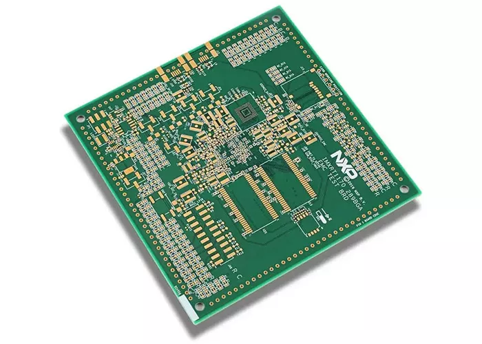
Multilayer PCB

Geyuan Electronics is a high-tech PCB manufacturer capable of supporting multilayer boards up to 60 layers, providing high-quality multilayer PCBs designed for high-density routing and stable signal integrity. As a reliable multilayer PCB supplier, we combine DFM feedback centered on stack-up structure with controlled lamination and drilling processes to support rapid prototyping, scalable production, and integrated PCB assembly services, all guaranteed by certified quality and efficient production processes.

Geyuan Electronics Boasts Over 20 Years Of Experience In Multilayer PCB Projects

With over 20 years of experience in the EMS field, Geyuan Electronics has accumulated expertise in handling complex multilayer PCB projects, particularly excelling at providing high-precision designs for demanding applications. To date, we have completed over 50,000 multilayer PCB manufacturing and assembly projects, consistently delivering high-quality results with rapid turnaround times. Our commitment to excellence has earned us a 99.50% customer satisfaction rate, thanks to efficient processes and clear communication, which fosters long-term partnerships.

Rapid prototyping of metal based multilayer PCBs

Multilayer PCB Types We Can Produce

Geyuan Electronics manufactures a wide variety of multilayer PCBs to meet the mechanical, electrical, and assembly requirements of your projects. From standard rigid multilayer boards to flexible and rigid-flex hybrid structures, our team can help you choose the most suitable multilayer PCB structure for your application.

Standard Multilayer PCBs

Standard Multilayer PCBs

These multilayer PCBs are the most prevalent kind, and a variety of electronic systems and gadgets use them. They can have anywhere between 4 and 20 layers and are made up of numerous layers of laminated conductive and non-conductive materials.
Rigid Multilayer PCBs

Rigid Multilayer PCBs

Rigid multilayer PCBs are the most widely used choice for products requiring stable structures, reliable interconnects, and consistent electrical performance. Geyuan Electronics manufactures rigid multilayer PCBs in various layer counts, materials, and stack-up structures.
Flexible Multilayer PCBs

Flexible Multilayer PCBs

Flexible multilayer PCBs are designed for applications requiring bending, folding, or mounting in confined spaces. We manufacture multilayer flexible PCBs using a polyimide-based structure to achieve compact designs, reduced wiring complexity, and increased assembly flexibility.
Rigid Flexible Multilayer PCBs

Rigid-Flexible Multilayer PCBs

Rigid-flex multilayer PCBs combine rigid portions for component mounting with flexible portions for interconnects within a single board structure. Geyuan Electronics provides rigid-flex multilayer PCB manufacturing services for applications requiring space savings, increased reliability, and enhanced resistance to vibration and mechanical stress.
HDI Multilayer PCBs

HDI Multilayer PCBs

HDI multilayer PCBs are designed for high-density designs that require finer traces, smaller vias, and more complex routing within limited board space. We provide HDI multilayer PCB manufacturing services for projects requiring compact layouts, higher I/O density, and better signal performance.
Metal Based Multilayer PCBs

Metal-Based Multilayer PCBs

Metal-based multilayer PCBs are suitable for applications with high requirements for thermal performance and thermal stability. Geyuan Electronics provides metal-based multilayer PCB solutions for power electronics, LED systems, and other products with high thermal management requirements.
High Frequency Multilayer PCBs

High-Frequency Multilayer PCBs

High-frequency, high-speed multilayer PCBs are used in designs where signal integrity, impedance control, and material properties are critical. We provide manufacturing support for high-frequency, high-speed multilayer PCBs for applications with higher electrical requirements, such as RF, microwave, telecommunications, and high-speed digital applications.
Lightweight Multilayer PCBs

Lightweight Multilayer PCBs

We have made rapid progress in the research and development and market launch of lightweight multilayer printed circuit board (PCB) assemblies, mastering the technology to stack multilayer circuit boards without taking up too much space. We continue to shrink the size of circuit boards, creating lightweight multilayer PCBs.
4 Layer Multilayer PCB

4 Layer PCB

Cost-effective multilayer solution ideal for consumer electronics, IoT products, and embedded systems.
6 Layer multilayer PCB

6 Layer PCB

Balanced performance for industrial control systems, automotive ECUs, and mixed-signal applications.
8 Layer Multilayer PCB

8 Layer PCB

Optimized for networking equipment, DDR memory routing, and telecom infrastructure systems.
10 Layer Multilayer PCB

10 Layer PCB

Designed for demanding applications requiring controlled impedance and high-density routing capability.
12 Layer Multilayer PCB

12 Layer PCB

Sequential lamination and HDI technology for servers, storage, and telecom backplanes.
14 Layer Multilayer PCB

14 Layer PCB

Ultra-complex routing architecture supporting multiple voltage domains and high-speed backdrill structures.
14 Layers Multilayer PCB

14+ Layers PCB

Custom high-layer-count PCB solutions for AI computing, military systems, data centers, and advanced networking.
16 24 Layer PCB

High-quality Multilayer PCB Prototyping And Rapid Mass Production

We are dedicated to serving you, regardless of order size. We possess expertise in producing high-tech printed circuit boards quickly and reliably. Depending on your needs, we can complete small-batch production within 1-2 days or mass production within just 5 days. To obtain a quote and order circuit boards, please send your design files via email or form. We offer 24/7 customer service and an engineering team ready to assist you and ensure your project gets off to a smooth start.

Multilayer PCB Technology Capabilities

MaterialFR4 (140Tg, 170Tg, 180Tg), Halogen-free, Metal Core, Polyimide, Rogers 4350B/3003/4003C/5880, Taconic, Teflon, Mix-Lamination, etc
Material BrandsKB, ITEQ, SY, ISOLA, Rogers (Arlon), Ventec, Laird, Nelco, Bergquist, DENKA, Panasonic, Taconic, or other laminate on customer’s request
Layer Count1~40
FlammailityUL 94V-0
Thermal Conductivity0.3W-400W/mk
Quality StandardsIPC Classes 2/3
HDI Build-upAny Layer, up to 4+N+4
Board Dimension1-2 Layers: 1500mmx600mm Multilayer: 620mmx720mm
Board Thickness0.037mm-6.5mm
Min Thickness2-layer: 0.1mm 4-layer: 0.4mm 6-layer: 0.6mm 8-layer: 0.8mm 10-layer: 1mm More than 10 layers: 0.5*Layer Count*0.2mm
Copper Thickness1/3~33oz
Solder Mask ColorsWhite, Black, Green, Blue, Red, Yellow, Orange, Purple, Matte Green, Matte Black
Solder Mask BrandsGreen: RongDa, KuangShun White: Coants, LanBang, Taiyo
Solder Mask Thickness0.2mil-1.6mil
Solder Mask Dam50μm
Surface FinishesBare Copper, Hasl lead-free, Carbon Ink, ENIG, Gold Fingers, OSP, IAg, ISn, etc
Plating ThicknessHASL: Copper Thickness: 20-35um Tin: 5-20 um Immersion Gold: Nickel: 100u”-200u” Gold: 2u” -4u” Hard Plated Gold: Nickel: 100u”-200u” Gold: 4u”-8u” Golden Finger: Nickel: 100u”-200u” Gold: 5u”-15u” Immersion Silver: 6u”-12u” OSP: Film 8u”-20u”
Min Hole SizeLaser: 0.08mm Mechanical: 0.15mm
Min Trace Width/Spacing64μm/64μm
Minimum Solder Mask Clearance2mil
Min Annular Ring50μm
Min Pad to Pad Clearance40μm
Via Plugging0.2~0.8mm
Line Width/Space Tolerance±0.015mm
Board Thickness Tolerance±5%
Hole Diameter Tolerance±0.05mm
Hole Location Tolerance±2mil
Layer to Layer Registration≤100μm
S/M Registration≤38μm
Aspect RatioStandard: 25:1 Max.: 35:1
Blind Vias Aspect Ratio0.8:1
Outline Tolerance±0.1mm
V- CUT Tolerance±10mi
Bevel Edge± 5mil
Impedance & Tolerance50Ω;±10%
Warp and Twist≤0.50% (max cap)
Quality TestAOI, 100% E-test
Value-Added ServicesDFM Check, Expedited Production (24Hrs)
Featured ProcessesZ-axis Milling, Thick Copper, Copper Block Embedded, High-Frequency Foam Board, High-Frequency Mix-Lamination, Blind/Buried Via, Press-Fit Hole, Castellated Holes, Step Staggered, Resin Plugged Hole, Countersink/Counterbore Hole, Via in Pad, Edge-Plating, Impedance Control, Carbon Ink, Peelable Solder Mask, Gold Finger
Data FormatsGerber, DXF, PCBdoc, ODB++, HPGL, BRD, etc
CapabilitiesDaily 3750 Sqm Monthly 110,000 Sqm
 
China Mainland Base
Turnkey ServiceDesign + PCB FAB + Components Sourcing + PCB Assembly + Product Assembly
Assembly TechnologiesTHT, SMT, Hybrid Mount, Subsystem Assembly
Manufacturing AbilitiesPrototyping, Low to High Volume
Component AbilitiesChips 0201mm BGA, QFP & CSP 0.25mm BGA repair and reball
SMT Lines11 Lines, Samsung / JT
SMT CapabilitiesMonthly 788 Million Points
THT Lines3 Lines, Auto / Manual
Inspection MachinesSPI, AOI, 2D X-Ray
TestingICT/Function test/Burn-in test/Aging Testing
Assembly CostLower Costs
Lead TimeAs fast as 9 days with shipping
Number of layersS<1m²1≤S<5m²5≤S<20m²20≤S<50m²50≤S<100m²100m²以上Expedited (≤3㎡)
2L45-75-76-98-109-1212~24 hours
4L56-86-88-1010-1210-151~4 working days
6L66-86-88-1010-1210-152~4 working days
8L76-86-88-1010-1210-154~6 working days
10L99-119-1110-1212-1413-175~9 working days
12L1010-1210-1211-1313-1514-187~14 working days
14L1010-1210-1211-1313-1514-187~14 working days
16L111313151617Contingent
18L121414161718Contingent
20L131414161819Contingent
22L151515182022Contingent
24L151515182022Contingent
26L151515182022Contingent
28L+151515182022Contingent
4 Layer PCB

Engineering Team and DFM Analysis Capabilities

Our engineering team possesses extensive knowledge and experience. We bring together experts in electrical, mechanical, and thermal design, working closely with our clients to ensure that every aspect of multilayer PCB design is optimized for performance and manufacturability. This collaborative approach allows us to proactively address potential challenges and incorporate client feedback throughout the design phase. Furthermore, Design for Manufacturability (DFM) is a critical component of our process. We ensure that designs are not only technically feasible but also economically viable. By considering manufacturing constraints and capabilities early in the design process, we mitigate the risk of production issues and ensure a smooth transition from design to production.

Customized Multilayer PCB Design and Manufacturing Solutions

Customization is at the heart of our PCB manufacturing business. We understand that every project presents unique challenges and requirements. Regardless of the type of multilayer PCB, our team can provide customized design and manufacturing solutions tailored to your specific needs. Leveraging advanced software tools, a streamlined design process, and a highly knowledgeable engineering team, we help clients transform complex designs into reliable, mass-producible solutions. Our manufacturing process integrates advanced equipment, premium materials, and rigorous quality control to ensure that every multilayer board fully meets design requirements. From early prototyping to mass production, we maintain consistently high standards, ensuring that every batch achieves the same level of quality.

Workers at Geyuan Electronics are soldering multilayer PCB boards
Multilayer PCB after assembly

Experienced Multilayer PCB Manufacturer

Geyuan Electronics, a multilayer PCB manufacturer with over 20 years of market experience, has the privilege of collaborating with numerous clients worldwide. This has helped us accumulate extensive expertise and build a strong brand image in the field. We have also established a robust supplier network and a streamlined supply chain process, ensuring timely and accurate sourcing of necessary components. With an on-time delivery rate exceeding 98%, we ensure our clients can rely on us for a stable and timely supply of multilayer PCBs to meet their project needs. Furthermore, we invest heavily in R&D and advanced technologies to enhance our capabilities. This, in turn, helps our clients maintain a leading position in product technology advancement.

Get a Quote for Your Multilayer PCB Project

Geyuan Electronics provides custom multilayer PCB manufacturing for customers who need reliable quality, engineering support, and stable production capability. Send your Gerber files and project requirements to receive a quotation and manufacturing review.

Call to Actions1
Multilayer PCB Internal structure display

Multilayer PCB Manufacturing Capabilities

Our multilayer PCB manufacturing capabilities are built upon precise, stable, and mature manufacturing technologies. With over two decades of practical experience, we can meet complex design requirements demanding stringent tolerances, reliable performance, and durability. Our services ensure that every product begins with actual DFM (Design for Manufacturability) and stack-up review to address critical risks early on, such as layer alignment, via configuration, copper balancing, and impedance-critical routing. Our process flow includes inner layer imaging/etching, controlled lamination, drilling and copper plating, and outer layer patterning, culminating in inspection and electrical testing to ensure consistent quality. We support high-mix prototyping and scalable small-to-medium volume production, guaranteeing consistency from prototype to mass production.

Additive Manufacturing for Multilayer PCB

With our additive manufacturing systems and processes, we can offer complex multilayer PCBs which have high component density and allows for miniaturization of appliances at competitive costs. Low-volume, high-complexity production and rapid prototyping of complex electronics is now made easy! Our team of experts possesses the necessary expertise and industry best practices to ensure you don’t encounter costly mistakes in any type of multilayer PCB manufacturing service.

High quality Multilayer PCB Prototyping

Multilayer PCB Manufacturing Process

Multilayer PCB manufacturing requires precise control at every stage, from engineering review and inner layer fabrication to lamination, drilling, electroplating, and final inspection. At Geyuan Electronics, we rigorously manage each step to ensure consistent layer alignment, reliable interconnects, and consistent board quality to meet the demanding requirements of multilayer PCB applications.

1. Engineering Review

This process begins with an engineering review of design data, stack-up requirements, and manufacturing details before production begins. This step helps confirm manufacturability, mitigate avoidable risks, and prepare for stable multilayer PCB manufacturing.

2. Material Preparation

Appropriate substrates, such as FR4, high Tg materials, polyimide, or other specified laminates, are selected based on the board structure and project requirements. Material preparation is a crucial step in ensuring the board meets mechanical, electrical, and thermal performance requirements.

3. Inner Layer Fabrication

Before lamination, the inner layers need to be imaged and etched to form the desired circuit patterns. Precision at this stage is critical because the inner layers determine much of the routing, power distribution, and grounding structure of the final multilayer PCB.

4. Lamination and Drilling

The treated copper layers and prepreg are laminated under controlled temperature and pressure to form a single multilayer structure. After lamination, drilling is performed to create vias and holes to achieve electrical interconnection between the layers.

5. Electroplating and Outer Layer Finishing

Electroplating is used to build conductive connections through vias, while simultaneously processing the outer layers to form the final circuit pattern. This stage directly affects interlayer connectivity, wiring accuracy, and the overall electrical performance of the circuit board.

6. Solder Mask and Surface Finishing

A solder mask is applied to protect the circuitry and reduce the risk of short circuits or contamination during assembly and use. Then, depending on product and assembly requirements, surface finishes such as lead-free HASL, ENIG, immersion silver, immersion tin, or hard gold are applied.

7. Electrical Testing and Final Inspection

Multilayer PCBs undergo electrical testing and final inspection before shipment to verify connectivity, detect faults, and confirm overall manufacturing quality. Depending on the project, inspections may include AOI (Automated Optical Inspection), flying probe testing, impedance testing, and other verification steps.

8. Packaging and Shipping

Our controlled packaging and shipping services help ensure that every multilayer PCB arrives safely in your hands. For more specific packaging requirements, Geyuan Electronics' packaging and shipping team can further meet your needs based on your design documents.

Mass production and assembly of multilayer PCBs

A Leading Multilayer PCB Supplier

Over 10,000 engineers and 500 contract assemblers worldwide trust Geyuan Electronics’ multilayer PCB manufacturing services. As a professional multilayer PCB supplier, we pride ourselves on our unwavering commitment to quality and consistently providing fully functional products that meet and exceed your requirements. Whether you need a simple double-sided FR4 board or a highly complex multilayer PCB, our PCB design and manufacturing experts can meet your needs and provide fast, efficient, and economical prototyping and high-volume production services with no hidden costs, assisting you through the transition from prototype to mass production. Contact us today to discuss your multilayer PCB prototyping and high-volume production needs with our service team.

Geyuan Electronics' Multilayer PCB Manufacturing and Testing Equipment

Geyuan Electronics’ in-house factories in Shenzhen and Dongguan, China, cover 12,400 square meters, including a 2,600-square-meter cleanroom, 5 SMT production lines, and 3 DIP production lines. We are equipped with precision drilling machines, electroplating systems, and etching equipment for accurate circuit patterning, as well as reflow soldering machines and wave soldering systems. Our advanced X-ray and AOI equipment ensures high-quality PCB production. Furthermore, we invest heavily in R&D of production equipment and processes each year, striving to keep pace with the latest developments in PCB manufacturing technology. Therefore, we have also introduced German BURKLE vacuum laminators and other supporting equipment, forming a high-precision multilayer PCB lamination production line.

Multilayer PCB Fabrication
Prototype sample assembled from multilayer boards

Cutting-Edge Technologies

Our advanced factory handles high-precision industrial control boards and flexible multilayer PCB for wearables, specializing in high-speed placement of fine-pitch components like SMD, BGA, and QFN.

  • From FR4 to Rogers to Metal Core
  • Up to 6-layer flexible circuits and rigid-flex designs
  • 64μm trace width/spacing for compact multilayer PCB
  • High-frequency, RF, high-power, and HDI support
  • SMT, THT, and hybrid assembly technologies
  • PCB 220k m²/month with PCBA 15M SMT points/day

From Prototyping to Mass Production

Geyuan Electronics supports the entire lifecycle of multilayer PCBs, from rapid prototyping to scalable mass production, enabling you to confidently transition from early validation to stable manufacturing. Our multilayer PCB manufacturing processes are designed to maintain consistent stack-up, repeatable via integrity, and proven electrical performance as volume increases.
We support engineering prototyping, mixed-variety assembly, and small-to-medium volume production, with adjustable scheduling and manufacturing controls to meet project timelines while ensuring quality. Our agile manufacturing model supports:

NPI (New Product Introduction) Programs

Structured support for early-stage designs and production ramp-up.

Design Validation with Rapid Feedback

DFM-focused feedback to improve manufacturability and reduce iterations.

Low- and High-Mix Production Volumes

Flexible multilayer PCB production aligned to varying complexity and demand.

Accelerated Time-to-Market

Streamlined workflows that shorten the transition from prototype to production.

Manufacturability Optimization During Design

Practical guidance on stackup, via structures, and fabrication constraints to improve yield and stability.

multilayer pcb manufacture

End-to-End Solutions

At Geyuan Electronics, we offer tailored solutions for multilayer PCB projects, ranging from complete turnkey services that reduce your operational workload to semi-turnkey options that provide greater flexibility.

  • Engineering Support
  • PCB Fabrication
  • PCBA Assembly
  • Box Build / System Integration
  • Testing & Validation
  • Supply Chain & Logistics

Quality at Every Step

Each multilayer PCB build follows defined inspections and documented process controls to ensure accuracy, consistency, and repeatability across prototypes and production runs.

  • Comprehensive Quality Control Systems: Standardized inspection procedures and real-time process monitoring across critical multilayer fabrication steps.
  • In-Process Inspection & Process Monitoring: Inner-layer imaging checks, lamination/registration control, and drilling/plating verification to reduce variation and protect yield.
  • Electrical Testing (E-Test): Electrical verification to detect opens/shorts and confirm connectivity before shipment.
  • Traceability & Documentation: Controlled build records and inspection documentation to support transparency and customer requirements.
  • Continuous Improvement Practices: Ongoing process optimization through internal review, training, and disciplined manufacturing execution.
Rapid prototyping of multilayer PCBs

Browse Different PCB Solutions for Every Need

Looking for the right PCB solution? Explore various types of PCBs to find the perfect match for your project.

Aluminum PCB

Aluminum PCB

PCBs with aluminum metal core for efficient heat dissipation in high‑power designs.
Single sided Rigid PCB

Rigid PCB

Standard rigid FR4 boards offering stable structure for general electronic systems.
Copper‑Core PCB

Copper‑Core PCB

Metal‑core PCB with copper base for superior thermal conductivity and heat spreading.
High Frequency PCB

High Frequency PCB

PCBs designed to handle signals in the GHz range with minimal signal loss and distortion.
High Speed PCB

High Speed PCB

Circuit boards optimized for high-speed digital signals with careful attention to signal integrity.
HDI PCB

HDI PCB

High Density Interconnect PCBs with finer lines, smaller vias, and higher connection density.
Rogers PCB

Rogers PCB

PCBs manufactured using Rogers Corporation's high-performance laminate materials.
Heavy Copper PCB

Heavy Copper PCB

PCBs with exceptionally thick copper layers, typically 3 oz or more, for high-current applications.
Flexible PCB

Flexible PCB

Bendable PCBs made with polyimide or polyester substrates for dynamic or space-constrained designs.
Rigid Flex PCB

Rigid-Flex PCB

Hybrid circuit boards that combine rigid and flexible substrates into a single integrated assembly.
Ceramic PCB

Ceramic PCB

Using ceramic substrates like Al₂O₃ and AlN for extreme thermal and electrical performance.
High TG PCB

High-TG PCB

PCBs made with high glass transition temperature (Tg) materials, typically 170°C and above.
Multilayer PCB small batch production

Manufacturing Process Control

  • Full BOM and lot traceability across production
  • Material traceability (components, boards, solder paste, etc.)
  • Process documentation for regulated manufacturing
  • First Article Inspection (FAI) support
  • In-process quality checks and monitoring
  • Controlled ESD & cleanroom processes (if applicable)
  • Complete inspection records and test reports
  • Change control and nonconformance management

Certification Compliance Support

  • Support for ISO 9001 quality management system
  • Compliance with ISO 14001 environmental management system
  • Adherence to ISO 45001 occupational health and safety standards
  • Compliance with IPC-A-610 and IPC J-STD-001 standards
  • Support for RoHS / REACH environmental compliance
  • Support for UL and CE certifications
  • Support for ISO 13485, IEC 62031, and other industry-specific certifications
Multilayer PCB products

Advanced Testing for Maximum Reliability

Reliable multilayer PCB performance requires not only precise manufacturing processes but also verification. Geyuan Electronics integrates inspection and electrical testing into the multilayer PCB manufacturing process to detect defects early and ensure boards meet manufacturing and electrical requirements. Our testing is suitable for prototypes and small to medium batch production; specific testing methods depend on stack-up complexity, number of layers, via configuration, and performance requirements. For impedance-controlled or high-reliability products, additional verification steps can be added to improve consistency. Our testing and inspection capabilities are as follows:

100% Electrical Testing (E-Test)

Verifies continuity and isolation to identify opens, shorts, and netlist-related issues before shipment.

Automated Optical Inspection (AOI)

Inspects outer-layer features to detect trace defects, spacing issues, and pattern irregularities.

Impedance Verification

Supports designs with controlled impedance targets by validating manufacturing consistency against impedance requirements.

Microsection / Cross-Section Analysis

Evaluates internal build quality—such as plating, layer registration, and via integrity—for higher reliability programs.

Final Visual Inspection

Confirms artistry, surface finish condition, and overall conformance to build requirements.

X-RAY

confirms buried-via fill and internal alignment a surface check can’t see

Industries and Applications We Support

Geyuan Electronics provides multilayer PCB manufacturing services for applications with extremely high requirements for wiring density, electrical performance stability, and manufacturing quality. We possess strong capabilities to support complex multilayer structures used in harsh environments, handling everything from rapid prototyping to scalable production. Through rigorous process control and electrical verification, our delivered multilayer PCBs fully meet the technical requirements of specific applications.

Industrial Equipment industry

Industrial & Automation

Wireless communications

Communications & Networking

Medical Electronics

Medical Electronics

New Energy

Energy & Power Systems

Consumer Electronics

Commercial Electronics

Emerging Technologies

Emerging Technologies

FAQ

A multilayer printed circuit board (PCB) is a single-board circuit board composed of three or more conductive copper layers bonded together. Insulating prepreg and core material are filled between the layers, and interconnected via plated through-holes, blind vias, or buried vias. The inner layers add signal routing layers, as well as dedicated ground and power layers, which are not available on single-sided and double-sided boards, enabling higher density and controllable impedance.

Geyuan Electronics manufactures multilayer PCBs with a maximum of 4 to 32 layers, but we can produce PCBs with over 60 layers. Regarding board thickness, a standard 4-layer board is typically about 1.6 mm thick, while the thickness of our multilayer boards can vary from 0.6 mm to 3.2 mm depending on design requirements.

We recommend that you collaborate with our design team as early as possible. We will conduct a comprehensive Design for Manufacturability (DFM) review, provide feedback on layout optimization, and ensure your design specifications meet our production capabilities. This collaborative approach helps minimize errors and shorten time-to-market.

Yes. Geyuan Electronics provides a one-stop service from chip manufacturing to turnkey PCB assembly, including SMT, DIP and BGA surface mount technology (including BGA solder joint X-ray inspection), component sourcing through authorized distributors, and functional testing. Therefore, all aspects of the PCB assembly, from bill of materials to final test assembly, are completed under one roof. Please discuss the assembly scope during the inquiry phase to ensure that Design for Manufacturability (DFM) and test coverage are planned in sync with chip manufacturing.

We use a variety of high-quality substrates, but the choice of materials depends on the specific requirements of each project. We support almost all substrates, including FR4, halogen-free, metal core, polyimide, Rogers, Taconic, Teflon, hybrid lamination, etc.

We have multiple automated factories in Shenzhen and Dongguan, China, with a monthly production capacity of up to 220,000 square meters of PCBs and 15 million SMT placement points per day. Furthermore, we not only produce multilayer PCBs, but also almost all types of PCBs.

Looking For An Expert Solution For Your Company?

Geyuan Electronics specializes in higher layer count PCBs, exotic materials, laser drill micro-vias, blind/buried vias, as well as conductive and non-conductive via fill. If you have any queries regarding to our multilayer PCB assembly service or need an urgent assistance, then please don’t hesitate to contact our team of skilled personnel’s.

Call to Actions1
Scroll to Top